
製品情報モノクログラフィックモジュール 128x64ドット
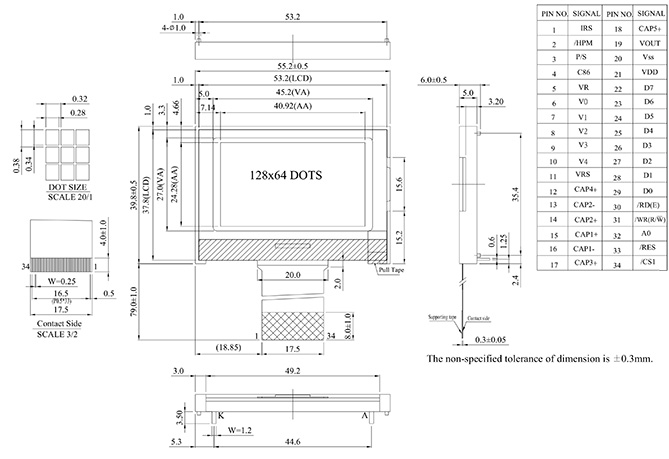
図面
特長
- VAサイズ:2.07インチ
- 画素数:128 x 64
- 供給電源:3.0V
- インターフェース:8ビットパラレル
- バックライト: White LED
- タッチパネルオプションなし
- COGモノクロ モジュール
- コネクタ接続
- RoHS対応
機械的仕様
- 外形サイズ:55.2(W) x39.8(H) x 6.0(T) mm (B/L含む)
- ビューイングエリア:45.2(W) x 27.0(H) mm
- アクティブエリア:40.92(W) x 24.28(H) mm
- ドットピッチ:0.32 x 0.38 mm
電気的特性
- 供給電圧:3 .0V
- 供給電流:1.0mA
- B/L電圧: 3.5V ( White LED B/L)
- B/L電流: 48mA (White LED B/L)
I/Fピン配置
| PIN NO. | Symbol | Level | Description |
|---|---|---|---|
| 1 | IRS | I | This terminal selects the resistors for the V0 voltage level adjustment. IRS = “H”: Use the internal resistors IRS = “L”: Do not use the internal resistors. The V0 voltage level is regulated by an external resistive voltage divider attached to the VR terminal |
| 2 | /HPM | I | This is the power control terminal for the power supply circuit for liquid crystal drive. /HPM = “H”: Normal mode /HPM = “L”: High power mode |
| 3 | P/S | I | This is the parallel data input/serial data input switch terminal. P/S = “H”: Parallel data input. P/S = “L”: Serial data input. When P/S = “L”, D0 to D5 fixed “H”. /RD (E) and /WR (R/W) are fixed to either “H” or “L”. With serial data input, It is impossible read data from RAM |
| 4 | C86 | I | This is the MPU interface selection pin. C86 = “H”: 6800 Series MPU interface. C86 = “L”: 8080 Series MPU interface |
| 5 | VR | I | Output voltage regulator terminal. Provides the voltage between VSS and V0 through a resistive voltage divider. IRS = “L” : the V0 voltage regulator internal resistors are not used. IRS = “H” : the V0 voltage regulator internal resistors are used. |
| 6~10 | V0~V4 | Power Supply | This is a multi-level power supply for the liquid crystal drive. |
| 11 | VRS | Power Supply | This is the internal-output VREG power supply for the LCD power supply voltage regulator. |
| 12 | CAP4+ | O | DC/DC voltage converter. Connect a capacitor between this terminal and the CAP2N terminal. |
| 13 | CAP2- | O | DC/DC voltage converter. Connect a capacitor between this terminal and the CAP2P terminal. |
| 14 | CAP2+ | O | DC/DC voltage converter. Connect a capacitor between this terminal and the CAP2N terminal. |
| 15 | CAP1+ | O | DC/DC voltage converter. Connect a capacitor between this terminal and the CAP1N terminal. |
| 16 | CAP1- | O | DC/DC voltage converter. Connect a capacitor between this terminal and the CAP1P terminal. |
| 17 | CAP3+ | O | DC/DC voltage converter. Connect a capacitor between this terminal and the CAP1P terminal. |
| 18 | CAP5+ | O | DC/DC voltage converter. Connect a capacitor between this terminal and the CAP1P terminal. |
| 19 | VOUT | O | DC/DC voltage converter. Connect a capacitor between this terminal and vss or VDD |
| 20 | VSS | Power Supply | Ground |
| 21 | VDD | Power Supply | Power supply |
| 22~29 | D7~D0 | I/O | Data bus line |
| 30 | /RD(E) | I | • When connected to 8080 series MPU, this pin is treated as the “/RD” signal of the 8080 MPU and is LOW-active. The data bus is in an output status when this signal is “L”. • When connected to 6800 series MPU, this pin is treated as the “E” signal of the 6800 MPU and is HIGH-active. This is the enable clock input terminal of the 6800 Series MPU. |
| 31 | /WR(RW) | I | • When connected to 8080 series MPU, this pin is treated as the “/WR” signal of the 8080 MPU and is LOW-active. The signals on the data bus are latched at the rising edge of the /WR signal. • When connected to 6800 series MPU, this pin is treated as the “R/W” signal of the 6800 MPU and decides the access type : When R/W = “H”: Read. When R/W = “L”: Write. |
| 32 | A0 | I | This is connect to the least significant bit of the normal MPU address bus, and it determines whether the data bits are data or command. A0 = “H”: Indicates that D0 to D7 are display data. A0 = “L”: Indicates that D0 to D7 are control data. |
| 33 | /RES | I | When RES is set to “L”, the setting are initialized. |
| 34 | /CS1 | I | This is the chip select signal. |
「モノクログラフィックモジュール 128x64ドット」のご相談やお見積もりをご希望のお客様は、こちらのフォームをご利用ください。
モノクログラフィックモジュール 関連製品ページメニュー
- No1. モノクログラフィックモジュール 96x49ドット
- No2. モノクログラフィックモジュール 98x64ドット
- No3. モノクログラフィックモジュール 128x32ドット
- No4. モノクログラフィックモジュール 122x32ドット
- No5. モノクログラフィックモジュール 122x32ドット
- No6. モノクログラフィックモジュール 122x32ドット
- No7. モノクログラフィックモジュール 122x32ドット
- No8. モノクログラフィックモジュール 122x32ドット
- No9. モノクログラフィックモジュール 128x64ドット
- No10. モノクログラフィックモジュール 128x64ドット
- No11. モノクログラフィックモジュール 128x64ドット
- No12. モノクログラフィックモジュール 128x64ドット
- No13. モノクログラフィックモジュール 128x64ドット
- No14. モノクログラフィックモジュール 128x64ドット
- No15. モノクログラフィックモジュール 128x64ドット
- No16. モノクログラフィックモジュール 128x64ドット
- No17. モノクログラフィックモジュール 128x64ドット
- No18. モノクログラフィックモジュール 128x64ドット
- No19. モノクログラフィックモジュール 128x64ドット
- No20. モノクログラフィックモジュール 128x64ドット
- No21. モノクログラフィックモジュール 128x64ドット
- No22. モノクログラフィックモジュール 128x128ドット
- No23. モノクログラフィックモジュール 128x128ドット
- No24. モノクログラフィックモジュール 160x128ドット
- No25. モノクログラフィックモジュール 160x160ドット
- No26. モノクログラフィックモジュール 240x64ドット
- No27. モノクログラフィックモジュール 240x64ドット
- No28. モノクログラフィックモジュール 240x64ドット
- No29. モノクログラフィックモジュール 240x128ドット
- No30. モノクログラフィックモジュール 240x160ドット
- No31. モノクログラフィックモジュール 320x240ドット
- No32. モノクログラフィックモジュール 320x240ドット
- No33. モノクログラフィックモジュール 320x240ドット
- No34. モノクログラフィックモジュール 320x240ドット
- No35. モノクログラフィックモジュール 320x240ドット
- No36. モノクログラフィックモジュール 320x240ドット
- No37. モノクログラフィックモジュール 320x240ドット